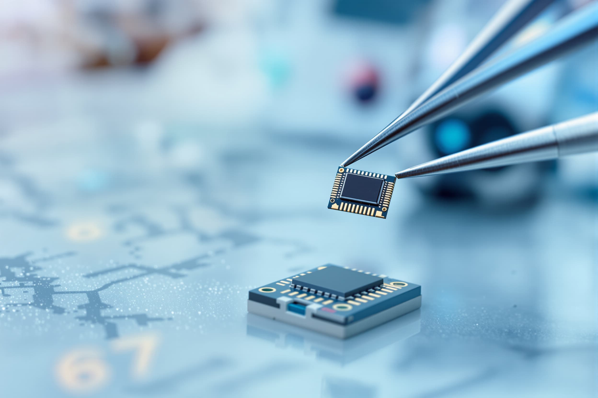
Microelectromechanical systems (MEMS) motion sensor combining accelerometer, gyroscope, and/or magnetometer functions in a package smaller than a pin head. Detects acceleration, rotation, and orientation changes, converting mechanical motion into electrical signals for consumer electronics. Components are as small as 4 microns, enabling ultra-compact low-power sensing.

Feasibility at a glance
PT localization
3/10
Low
Only finishing and testing can be localised in Portugal.
Per unit
€2–15
at 100000-unit volume
Starter batch
100,000units
minimum viable run
To first batch
32weeks
6 phases, design to ship
Budget
€180–320k
all-in estimate
Bottom line
MEMS motion sensors require extremely advanced semiconductor fabrication capabilities (4-micron photolithography, ASIC design, wafer-scale MEMS etching, wire bonding) that do not exist in Portugal. The only viable European path is co-development with established MEMS/semiconductor players like STMicroelectronics (France/Italy) or Bosch Sensortec (Germany), who possess the cleanroom infrastructure, IP, and process expertise. White-label is not feasible since MEMS sensors are typically application-specific and require integration engineering. Local production is impossible without multi-billion euro semiconductor fabs.
5 capabilities
Detects changes in motion, acceleration, and orientation by measuring how tiny mechanical structures shift inside the sensor.
Enables screen rotation on smartphones by sensing when you flip the device from portrait to landscape.
Stabilizes drone flight and altitude by continuously measuring tilt and movement in three dimensions.
Tracks fitness activities like steps, running, or cycling by recognizing specific motion patterns.
Reduces power consumption by waking devices only when real movement is detected.
5 stations · build route
Microfabricate MEMS structures on silicon wafer
Use photolithography and etching to create mechanical features as small as 4 microns—ten times thinner than a human hair.
Fabricate ASIC chip
Manufacture the companion signal-processing integrated circuit using standard semiconductor processes.
Die attach and wire bonding
Mount the MEMS die and ASIC inside the package, then connect them electrically with ultra-fine gold or aluminum wires.
Package encapsulation and molding
Seal the components in a compact LGA or similar surface-mount package, protecting them from moisture and mechanical stress.
Calibration and functional testing
Test each sensor on motion simulators to calibrate offsets, verify accuracy, and ensure it meets specification before shipping.
Microfabricate MEMS structures on silicon wafer
Use photolithography and etching to create mechanical features as small as 4 microns—ten times thinner than a human hair.
Fabricate ASIC chip
Manufacture the companion signal-processing integrated circuit using standard semiconductor processes.
Die attach and wire bonding
Mount the MEMS die and ASIC inside the package, then connect them electrically with ultra-fine gold or aluminum wires.
Package encapsulation and molding
Seal the components in a compact LGA or similar surface-mount package, protecting them from moisture and mechanical stress.
Calibration and functional testing
5 identified · 2 blocking
High
MEMS Foundry Capacity Shortage
The global MEMS market is highly concentrated, with fewer than 20 foundries capable of high-volume consumer-grade motion sensor production. During semiconductor shortages (like 2021–2023), MEMS capacity is allocated to strategic customers with multi-year agreements and high volumes. A startup or mid-volume customer risks being de-prioritized, leading to 6–12 month delays or complete inability to secure wafer starts. This risk is compounded if relying on a single foundry partner without second-source agreements.
Mitigation — Negotiate a multi-year volume commitment or framework agreement with the MEMS partner during initial co-development, even if it includes take-or-pay clauses. Secure allocation for at least 18 months of forecasted demand upfront. Establish a qualified second source (e.g., both STMicro and Bosch Sensortec) by designing to a standard footprint and interface (e.g., I2C/SPI, common LGA-14 package). Maintain 12–16 weeks of safety stock once production stabilizes.
High
Extended Lead Times and Prototype Iteration Delays
MEMS sensor development is inherently iterative. Initial samples often reveal issues in sensitivity, offset drift, temperature stability, or mechanical shock tolerance that require design tweaks—each iteration consuming 6–10 weeks (wafer lot cycle time) plus test and characterization. If the ASIC or MEMS structure requires a metal mask change, NRE costs of €20k–40k per spin are incurred. Cumulative delays can push time-to-market from 6 months to 12–18 months, jeopardizing product launch windows and competitive positioning.
Mitigation — Front-load design validation with extensive simulation (FEA for mechanical structures, SPICE for ASIC) and reference designs from the foundry partner. Request multi-corner process splits (fast/typical/slow) on the first wafer lot to characterize yield and performance margins. Plan for at least two prototype iterations in the project timeline and budget. Use known-good reference MEMS designs (e.g., catalog sensor as starting point for semi-custom) rather than clean-sheet development. Allocate 4–6 weeks of test and characterization time per prototype batch to catch issues early.
Medium
Intellectual Property and Design Leakage
MEMS sensor design involves valuable IP in mechanical structure geometry, ASIC algorithms (filtering, noise reduction, sensor fusion), and calibration coefficients. If working with a partner who also serves competitors or operates facilities in jurisdictions with weak IP enforcement, proprietary algorithms and design parameters could be reverse-engineered or leaked. This is especially risky if custom firmware or calibration routines are shared without adequate contractual protections.
Mitigation — Negotiate clear IP ownership and confidentiality clauses in the co-development agreement, specifying that all custom MEMS geometries, ASIC code, and calibration data remain GETMILK property. Use NDAs with financial penalties for breach. Keep high-value algorithmic IP (sensor fusion, motion pattern recognition) on the host microcontroller firmware rather than embedding it in the ASIC. Consider geographic IP registration (EU patents) and work only with Tier-1 partners who have strong compliance track records.
Medium
CE Marking and RED Compliance for Integrated Devices
Although the MEMS sensor itself is a passive component, when integrated into wireless devices (e.g., fitness trackers, drones, IoT nodes), the final product must meet Radio Equipment Directive (RED), EMC Directive, and RoHS/REACH substance restrictions. MEMS sensors can be sensitive to electromagnetic interference and require careful PCB layout and shielding. If the sensor is used in safety-critical applications (medical devices, automotive), additional functional safety standards (ISO 26262, IEC 62304) apply. Inadequate compliance testing can delay market entry by 3–6 months and incur costs of €20k–50k for re-testing and certification.
Mitigation — Engage a notified body or accredited test lab (e.g., TÜV, SGS, Intertek) early in the design phase to validate EMC performance and RED compliance test plans. Request RoHS/REACH declarations and conflict minerals reports from the MEMS supplier as part of the supply contract. Perform pre-compliance EMC testing on prototypes before committing to final production tooling. Budget €30k–60k and 8–12 weeks for full CE compliance testing and technical file preparation.
Medium
Calibration and Yield Variability in MEMS Production
MEMS sensors exhibit inherent unit-to-unit variation due to nanometer-scale fabrication tolerances. Without individual calibration (offset nulling, sensitivity trimming, temperature compensation), sensors can show ±10–20% accuracy variation, making them unsuitable for precision applications. High-volume calibration requires specialized motion simulators (rate tables, shake tables) and adds €0.50–2.00 per unit in test cost. Poor calibration processes or inadequate test coverage can lead to field failures, returns, and damage to brand reputation.
Mitigation — Specify calibration requirements (offset, sensitivity, cross-axis sensitivity, temperature coefficients) in the manufacturing agreement and require the foundry to perform multi-axis calibration and store coefficients in sensor OTP (one-time programmable) memory or EEPROM. Audit the foundry's calibration process and request Cpk data (process capability) showing >1.33 for critical parameters. Implement end-of-line testing on a sample basis (AQL 1.5 or better) to verify calibration accuracy. Budget €1.00–1.50 per unit for comprehensive calibration and test.
32 weeks to first batch
Specification Freeze and Partner Selection
wk 1–4MEMS and ASIC Design Phase
wk 5–14Wafer Fabrication and MEMS Etching
wk 15–23Die Attach, Wire Bonding, and Packaging
wk 24–26Calibration and Functional Test
wk 27–29First Production Batch and Validation
wk 30–32Specification Freeze and Partner Selection
MEMS and ASIC Design Phase
Wafer Fabrication and MEMS Etching
wk 5–14 is the longest stretch — MEMS and ASIC Design Phase takes 10 weeks of the 32 weeks on this build.
5 materials · 5 processes
Materials
Processes
354 Portuguese manufacturers matched
None cover the whole build — it splits across steps.
15 tasks · 13 weeks to first batch
Week 1
2 tasks
Freeze sensor specification and performance requirements
Document measurement range (±2g/±250°/s typical), power budget (<500µA active), package (LGA-14 or LGA-12), interface (I2C/SPI), and application context (fitness tracker, drone stabilization, etc.). Create technical requirements document for RFQ.
Issue RFQ to STMicro, Bosch Sensortec, and ams OSRAM
waits on Freeze sensor specification and performance requirements
Send technical requirements, volume forecast (100k/year), and timeline expectations. Request proposals covering NRE, per-unit cost, lead time, IP ownership terms, calibration support, and minimum order quantities.
Weeks 2–3
3 tasks
Evaluate foundry proposals and negotiate co-dev agreement
waits on Issue RFQ to STMicro, Bosch Sensortec, and ams OSRAM
Score proposals on cost, capability, IP terms, and support quality. Conduct technical deep-dive calls with top 2 candidates. Negotiate NRE payment terms (milestone-based), allocation guarantees, and IP ownership. Select partner and sign term sheet.
Engage compliance and test lab for CE/RoHS roadmap
waits on Evaluate foundry proposals and negotiate co-dev agreement
Contact TÜV, SGS, or Intertek to scope EMC, RoHS/REACH documentation, and RED testing if wireless integration planned. Request preliminary compliance gap analysis and testing timeline. Obtain RoHS/REACH declarations from selected foundry partner.
Secure legal review of co-development IP terms
waits on Evaluate foundry proposals and negotiate co-dev agreement
Have IP attorney review co-development agreement, focusing on ownership of custom MEMS geometries, ASIC firmware, calibration algorithms, and confidentiality clauses. Negotiate changes to protect GETMILK proprietary algorithms and ensure second-source freedom.
Weeks 4–7
3 tasks
Complete MEMS mechanical design and FEA simulation
waits on Evaluate foundry proposals and negotiate co-dev agreement
Work with foundry design team to specify spring-mass geometry, capacitive comb dimensions, and damping characteristics. Run finite-element analysis (FEA) to validate sensitivity, cross-axis rejection, and shock tolerance. Freeze mechanical design for mask set release.
Define ASIC architecture and interface specifications
waits on Evaluate foundry proposals and negotiate co-dev agreement
Specify charge amplifier gain, ADC resolution (12–16 bit), digital filter bandwidth, I2C/SPI register map, self-test modes, and power management. Review ASIC block diagram and SPICE simulations with foundry. Approve ASIC design for tape-out.
Release photomask set and initiate wafer fabrication
waits on Complete MEMS mechanical design and FEA simulation, Define ASIC architecture and interface specifications
Foundry completes mask tape-out for MEMS DRIE process and ASIC CMOS layers. Submit wafer lot orders (typically 25 wafers per lot). Track wafer lot through cleanroom with weekly status updates. Expect 8–10 week cycle time for first silicon.
Weeks 8–16
5 tasks
Develop firmware integration and calibration test plan
waits on Define ASIC architecture and interface specifications
Write I2C/SPI driver code for host microcontroller. Define calibration procedure (offset nulling, sensitivity scaling, temperature compensation). Prepare test scripts for motion simulator validation. Coordinate with foundry on calibration data format (OTP memory map).
Conduct wafer-level and package assembly
waits on Release photomask set and initiate wafer fabrication
Foundry completes wafer fabrication, dicing, die attach, wire bonding (8 bonds per sensor), and LGA molding. Perform in-line SEM inspection of MEMS structures and wire bond pull testing. Package first prototype batch of 500–1000 sensors for characterization.
Perform calibration and electrical characterization
waits on Conduct wafer-level and package assembly
Load prototype sensors onto 3-axis rate table and shake table. Measure offset, sensitivity, noise density, cross-axis coupling, and temperature drift. Program calibration coefficients into OTP memory. Generate characterization report and compare to specification targets.
Ongoing
2 tasks
Monitor wafer lot progress and escalate delays
waits on Release photomask set and initiate wafer fabrication
Hold bi-weekly status calls with foundry account team. Track wafer starts, cleanroom cycle time, and packaging queue. Escalate any capacity or yield issues immediately. Maintain risk register for supply allocation and second-source planning.
Establish quality agreement and incoming inspection
waits on Review prototype results and plan production ramp
Negotiate quality agreement covering AQL sampling (1.5 major, 0.65 critical), failure analysis, RMA process, and Cpk reporting (target >1.33). Set up incoming QC for first production batches: visual inspection, X-ray for wire bonds, parametric electrical test on 0.4% sample.
6 roles to fill before month one
STMicroelectronics, Bosch Sensortec, or ams OSRAM business development
MEMS Foundry Account Manager
Primary technical and commercial interface for co-development agreement, NRE negotiation, allocation guarantees, and escalation of capacity or yield issues. Critical for securing 100k-unit production slot and managing 28-week lead time.
Foundry or contract design house specializing in MEMS/ASIC integration
MEMS Design Engineer
Leads mechanical structure design (spring-mass geometry, comb drives), FEA simulation, ASIC architecture, and photomask tape-out. Essential for achieving 4-micron precision and meeting sensitivity/power specifications.
Foundry test operations or third-party motion simulator lab
Calibration & Test Engineer
Responsible for multi-axis calibration (rate table, shake table), programming OTP coefficients, electrical test development, and yield analysis. Ensures ±2% accuracy target and >90% production yield.
Notified body (TÜV, SGS, Intertek) for CE/RoHS/EMC certification
Compliance Specialist
Guides pre-compliance testing, EMC test planning, RoHS/REACH documentation, and RED certification if wireless. Avoids 3–6 month market entry delays and €30k–50k re-testing costs.
5 things to avoid in this plan
lead time
Lock in 18-month foundry allocation upfront—MEMS capacity shortages can delay wafer starts by 6–12 months; negotiate volume commitment or take-or-pay clause during co-dev agreement.
cost
Plan for two prototype iterations—first silicon rarely meets all specs; budget €40k and 10 weeks per spin for mask changes, wafer lot, and re-characterization.
supply
Secure second-source qualification by month 6—single-source dependency is catastrophic; design to common LGA footprint and interface so STMicro and Bosch parts are drop-in compatible.
watch-out
Front-load IP protection—specify in contract that GETMILK owns all custom MEMS geometries, ASIC code, and calibration data; keep sensor fusion algorithms on host MCU, not in ASIC.
cost
Budget €1.00–1.50 per unit for calibration—uncalibrated MEMS show ±10–20% variation; foundry must perform multi-axis calibration and program OTP memory, or field failures will destroy reputation.
2 tasks in week 1
Freeze sensor specification and performance requirements
Test each sensor on motion simulators to calibrate offsets, verify accuracy, and ensure it meets specification before shipping.
Die Attach, Wire Bonding, and Packaging
Calibration and Functional Test
First Production Batch and Validation
Launch pre-compliance EMC and environmental testing
waits on Perform calibration and electrical characterization
Submit prototype sensors to test lab for pre-compliance EMC (radiated/conducted emissions, ESD, burst). Conduct thermal shock (-40°C to +85°C), vibration (10g, 20–2000 Hz), and humidity (85%RH, 85°C) stress tests. Identify any design weaknesses for next iteration.
Review prototype results and plan production ramp
waits on Perform calibration and electrical characterization, Launch pre-compliance EMC and environmental testing
Analyze characterization data, yield metrics (target >90%), and test failures. Decide if design iteration is needed or if production release is approved. Negotiate production allocation (50k–100k units over next 6 months), payment terms, and delivery schedule with foundry.
EU-based law firm with MEMS and semiconductor IP expertise
IP Attorney (Electronics/Semiconductor)
Reviews co-development agreement to protect GETMILK ownership of custom MEMS designs, ASIC firmware, and calibration algorithms. Negotiates confidentiality terms and second-source freedom to mitigate IP leakage risk.
Contract or fractional ops lead with MEMS/semiconductor sourcing experience
Supply Chain Manager (Semiconductors)
Manages foundry relationship, negotiates multi-year allocation and take-or-pay terms, establishes second source, coordinates incoming QC, and maintains 12–16 week safety stock to mitigate capacity shortage risk.
354 matched · 8 shown, ranked by coverage
Covers, left to right: PCB Fabrication · SMT Assembly · Injection Molding · Testing & Inspection · Packaging
Manufacturer
Location
Covers
Certifications
People
Portuguese producers per required step
Testing & Inspection
178
Injection Molding
174
SMT Assembly
36
PCB Fabrication
6
Packaging
0
How many cover more than one step
The gap
MEMS motion sensors require extremely advanced semiconductor fabrication capabilities (4-micron photolithography, ASIC design, wafer-scale MEMS etching, wire bonding) that do not exist in Portugal. The only viable European path is co-development with established MEMS/semiconductor players like STMicroelectronics (France/Italy) or Bosch Sensortec (Germany), who possess the cleanroom infrastructure, IP, and process expertise. White-label is not feasible since MEMS sensors are typically application-specific and require integration engineering. Local production is impossible without multi-billion euro semiconductor fabs.
Send one RFQ to the top 4
Exatronic, Keenfinity EMS, Uartrónica, Proto-Electronics — same package, one click.